Reviving an Analog Polysynth with an Arduino, Ghidra, and Python
About a year ago, smack in the middle of the pandemic, I turned to the internet for some retail therapy. I’m a musician, so my usual retail therapist of choice is Reverb.com; a sort of fancy Craigslist or eBay just for musicians. Every day, I would see new listings pop up for instruments I might want, like a 6-string fan-fret bass, a nice electronic drum kit, or my “holy grail” - a super-rare, 22-year-old analog synthesizer: the Alesis Andromeda.

The Andromeda is a 16-voice polyphonic analogue synthesizer; basically a keyboard that sounds very lush, human, and organic, and can play a lot of notes at once. (That combination is expensive, for reasons.) Every function is controllable by a separate knob on the front panel, making it extremely interactive; every knob makes the sound change in some way.
As a kid, I remember playing one of these at my local music store in the early 2000s. It was the biggest, most expensive, and most intimidating thing in the shop. Here’s an extremely kitschy ‘90s demo video:
Synthesizers with similar capabilities cost over $9,000 today. The Andromeda was discontinued in 2010, and since then, prices for working units have shot up to around $6,000. There’s no way I could justify spending that kind of money.
Until one day, in October 2021, a listing popped up on Reverb. The seller was explicit: this unit was used, broken, and non-functioning.

I’m selling this synth for parts. It turns on but hangs on the splash screen. It’s missing side trim pieces, pitch/mod assembly, several knobs and several screws. The casing has nicks and scratches. The metal sides are a bit bent. The cable that connects the analog board to the main board has a cracked tensioner so maybe that’s part of the issue? I don’t have the tools or knowledge to fix this one so I’m passing it on. I can’t get it to do any tests so I can’t tell if anything is working. No returns on this one.
I was tempted. I looked up the service manual online, and found that there were many debugging steps one could take to try to fix problems like this. I’ve also had plenty of experience dealing with hardware. My computer hardware classes at university even dealt with the same CPU used by this synth - the Motorola Coldfire (which uses a variant of the M68k architecture) - and I had a small cache of tools that might be useful. Feeling bold, and desperately bored after 18 months of working from home, I sent an offer.

After two weeks of eager waiting, the synth arrived to my apartment in New York from Portland in a massive box. As described, it was in bad shape. The service manual provided a list of debugging functions that could be accessed by holding down one of eight buttons on the front panel during boot:

I had hoped that the previous seller just hadn’t discovered this information, but it turned out that these functions did not work at all. Time to dig deeper. No combination of buttons would do anything, nor would any other tips or tricks from the official manual.
RTFM (Read The Fancy Manual) #
Luckily, back in February of 2015, users on the popular forum GearSpace started a 15-page thread about how to debug a non-booting Andromeda. This thread included links to a confidential service manual that contained more debugging tips, intended for distribution only to Alesis-approved service centers. This service manual also included full schematics for the entire synth, showing how all of the components were logically connected together.

This service manual revealed a couple of important things: while this is an analogue synthesizer, meaning that sound is generated via non-digital, analogue circuitry, its brain is entirely digital. It uses a Coldfire CPU (an MCF5307 running at 90MHz), has 2MB of Flash memory to store its upgradeable operating system, 1MB of RAM for use at runtime, and 512kB of battery-backed RAM for persistent storage of user settings.
The great people in this thread also suggested a number of fixes to try:
Replacing the resonator on the LCD panel: the Andromeda will often fail to boot if the front panel controller can’t communicate with the LCD. The LCD panel uses a 3MHz ceramic resonator that can sometimes fail, and when the LCD’s clock is unstable, serial communication with it can fail. Luckily, a new crystal oscillator costs about $1, and that part is very easy to replace. (Unluckily, that didn’t seem to help.)
Adding a pull-up resistor to the SRAM chips: the Andromeda uses two external static RAM chips, providing a total of one megabyte of RAM. These external RAM chips are connected to the data and address busses of the CPU. During boot time, each SRAM chip may accidentally be enabled by default. If this happens, other devices on the bus (like the Flash memory chip that stores the operating system) will have their data overwritten by the data coming from each SRAM chip until they are disabled. (Think: too many people talking at once.)
This problem is called bus contention. The solution to this problem is to “tie” the Chip Enable pin of each chip to its “off” value (+3.3 volts) by using a resistor. This resistor is called a pull-up, as it pulls up the voltage on the pin when no other devices are controlling the line. By using a resistor, other devices are still able to pull the pin high or low; the resistor essentially sets a default value.
This resistor is a cheap and plentiful part - a 4.7kΩ resistor costs only pennies. Adding the resistor requires very careful soldering, though, as the pins on the SRAM chip are extremely close together. More on that later.
Replacing the Flash memory chip that stores the operating system. This logically made sense; Flash memory is reprogrammable, and it’s possible that the Flash may have been corrupted somehow, preventing the system from booting. Unfortunately, the Flash memory on the board is an extremely small part and is difficult to replace without advanced soldering skills or the proper equipment.
Replacing the entire CPU. I was incredulous about this; I’ve never heard of entire CPUs failing, but many people suggested that a whole-CPU replacement was necessary to get their synthesizers working again. This was a last-resort issue, as the CPU had 208 extremely fine pins that would be difficult to solder.
Breaking out the Soldering Iron #
At this point, I thought the next step was to start making changes to the hardware to try to fix one or more broken parts. I’ve been using a soldering iron on and off since I was about 10 years old, so I thought I had the dexterity, patience, and steady hand required to solder a single resistor across the two pins.
I did not.

In my effort to add a resistor between chip U12 and capacitor C50, I managed to short out multiple pins of U12. Then, when trying to fix my mistake by replacing the chip, I accidentally tore off at least 12 of the 44 solder pads that connect the chip to the circuit board.
If the synth wasn’t working before, it definitely wasn’t working now. I had to concede defeat and call in someone to help.
I started emailing around to local, NYC-area electronics repair shops - including the famed Rossmann Repair Group only blocks away, but none of them said they were able to fix a problem like this. After some more searching, I found a blog post from Edmonton-based VideogameRepairs.ca in which they had replaced the CPU and Flash chips of an Andromeda in the past, and sent them photos, asking if they would be able to fix my self-inflicted soldering damage. To my surprise, they said they’d be able to repair the board and replace its CPU, although had no means to test it.
Two months later, after buying a replacement CPU on eBay and shipping my main board from New York to Edmonton and back, I finally had a repaired board with a new SRAM chip and CPU. I had opted not to replace the Flash memory, as I didn’t know if it was good or bad, or how to go about reprogramming it. As part of the repair, a pull-up resistor was also added to the SRAM chips’ chip-select pin, just like the folks on Gearspace.com had suggested. (The repair job was amazing; huge thank you to Daniel Wynne at VideogameRepairs in Edmonton for such intricate rework - and for only $300 USD, too!)

…but the machine still refused to boot. Time to step things up a bit.
Breaking out the Debugger #
As I was waiting for my repaired circuit board to arrive in the mail, I pored through the service manual carefully. Surely there must have been some way to get more insight into what was going wrong during the boot process. The design engineers at Alesis included many test points in the synth where it was possible to hook up an oscilloscope or logic analyzer to ensure the system was behaving as expected.
Along with those test points, I noticed that the Coldfire CPU exposed a number of pins to a 26-pin header, conveniently labelled DEBUG PORT.

Some searching for some of the keywords on the circuit diagram - including DDATA and PST0 - led me to discover that this was a proprietary (but well documented) debugging interface specific to Coldfire processors. This is a form of debug interface known as Background Debug Mode, or BDM; which provides much of the functionality required by today’s software debuggers, like GDB or LLDB.
I spent a couple of days searching more to find any existing software and hardware that could connect to this debug port. Unfortunately, each solution was a pain, for different reasons:
- BDM interfaces exist on eBay for less than $20, but they target a slightly different BDM protocol than the one used by this CPU.
- Open-source projects like USBDM exist, but require custom hardware interfaces that don’t seem to be for sale anywhere, only seem to work on Windows and Linux, and require proprietary IDEs like CodeWarrior.
- PEMicro sells debug probes that are pin-compatible with exactly this Coldfire debug interface, but the cheapest hardware options cost $300. (This would have probably worked, to be honest.)
Building a BDM Interface #
Given that it was fairly difficult or expensive to use existing tools, I looked to see if maybe I could build my own using common parts, like an Arduino. The CPU’s 484-page user manual goes into tons of detail about how its debug port works: it’s really just a serial interface where the debugger sends one bit of information at a time over a single wire, while toggling a clock line to indicate when information is ready to be read. The CPU can then send data back to the debugger, also one bit at a time, by putting either 0V or 3.3V on its output line when the debugger toggles the clock line.
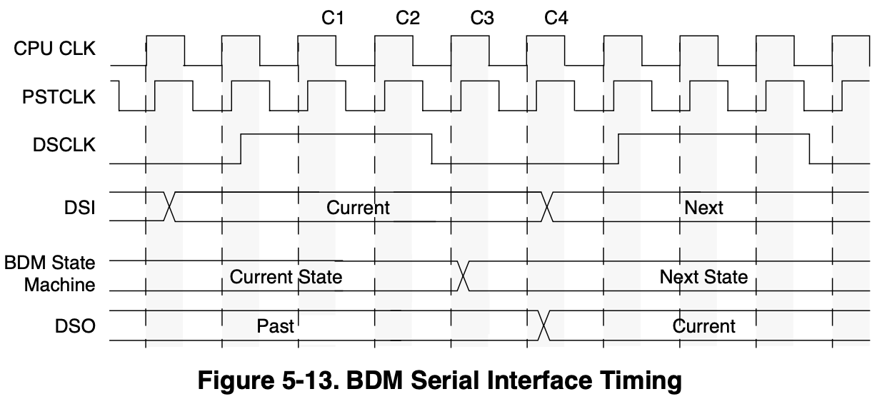
One very nice part of this serial interface is that it’s completely asynchronous: there are no timing requirements on either the debugger or the CPU. If the Arduino is busy doing something else, or is just slow (as Arduinos are) then the CPU doesn’t care - it just waits for the next bit to come in, one at a time.
On top of this serial interface, the Coldfire encodes its debug data into 17-bit packets - one bit (called the “status”) to indicate if an error has occurred, and 16 bits to indicate the data in that packet:

Then, on top of this packet format, different commands can be sent to the CPU to ask it to do things - like read or write memory addresses, read or write processor registers, continue processor execution, or put the processor into step mode.

With these operations, there’s enough there to build a rudimentary debugger: we can halt the processor, move the program counter where we want, read registers and memory, and watch as the operating system tries to boot.
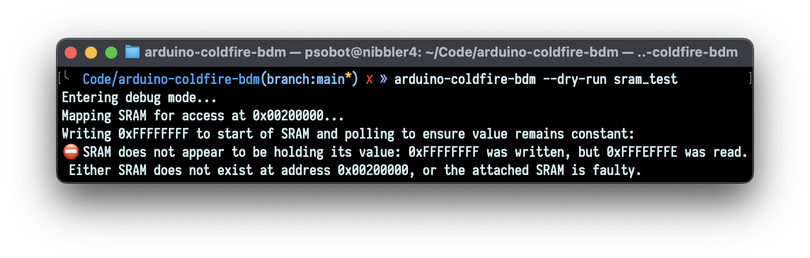
So, I wrote (and published!) a simple Python library called arduino-coldfire-bdm that encodes data and provides an interface to the Coldfire’s BDM port. A tiny Arduino program allows using pretty much any Arduino as a serial bridge between my laptop and the Andromeda’s CPU, so that we can send commands directly from Python to the board.
With that, we’re able to capture an execution trace to see what the processor is doing when it tries to boot, and it’s kinda neat: we can watch the program counter tick up!
And then the whole thing stops:

Turning to Ghidra #
Alright, now we’ve got an execution trace. We can watch the processor try to boot. And we can see that the processor gets a certain amount of the way through the process, and then halts.
To actually make sense of this without having to read assembly directly, I turned once again to Ghidra, the NSA’s open-source reverse engineering tool, which includes good support for the Coldfire architecture and allows us to decompile assembly code into C.
Unlike the last time that I wrote an extended blog post about using Ghidra, this experience was much simpler: the bootloader of the Andromeda is quite readable. I’ve annotated the boot code below, which also (pretty much) corresponds with the execution trace above:

Based on the execution trace, it seems the initial code runs for a bit - and then enters the loop at the bottom of this initial function, which copies the bootloader into RAM. Then, immediately after jumping to the code that was just copied into RAM, the processor halts immediately.
Well, that sounds suspicious. The code in RAM should be executable, but it seems that it’s either incorrect or didn’t get copied correctly. Let’s see if we can re-flash the bootloader firmware, to ensure that the code is correct.
Flashing the Flash in a Flash #
Flash memory seems like it’s all around us today; it’s what you find in SD cards, in your SSDs, and so on. Flash memory was novel when it first came out in the 1980s and 90s, as it was able to hold its contents without power, whereas other kinds of memory (like static RAM, or SRAM) required power to avoid having its contents fade away.
However, flash memory (or at least NAND flash, cheapest version) has a couple unexpected quirks that make it more complicated to use than regular RAM. A static RAM chip allows for reading and writing to any address just with a single read or write - functionally, by setting the address lines of the chip to the desired address, asserting one of the “write enable” or “output enable” signals, then either asserting the data on the data pins, or reading the data off of the data pins. Flash memory can be read the same way, but can only be written after sending special commands to the chip first.
Worse yet, bits in flash memory can only be switched from 1 to 0. To change a 0 to a 1, an entire block of memory (usually many kilobytes in size) must be “flashed” at once, setting all of that block’s bits to 1. After that erase operation is complete, individual bytes or words of memory can then be written one-at-a-time; but only by flipping 1 bits to 0.
All of this complexity means that if we want to reprogram the flash memory in the Andromeda, we’ll need to send a special sequence of commands to the CPU, rather than just asking it to write to memory. These commands are listed in the datasheet for each specific flash memory chip (although many chips share the same command sequences). The chip on the Andromeda main board responds to the commands in the following table from its datasheet:

What this somewhat hard-to-read table suggests is that to “program” (write) data to the flash memory, we need to send four individual writes to the memory chip: 0x555 = 0xAA, 0x2AA = 0x55, 0x555 = 0xA0, followed by a write directly to the address we want to place the data at. (This is presumably to prevent errant writes, as writing to flash memory would almost certainly result in corrupted data due to its inability to flip individual bits from 0 to 1.)
This is super slow, though. Sending four writes per word means that our writes actually go four times slower than they could, which - given how slow our custom BDM interface is - would result in us writing to the flash chip at a rate of only about 400 bytes per second. (It would take just over an hour to write just the bootloader at that rate.)
Luckily, this flash chip supports a feature its manufacturer calls “Unlock Bypass.” By sending a specific command to enter “Unlock Bypass” mode, writes can be performed by sending only two individual write commands instead of four. This doubles our writing speed, and allows us to upload the entire bootloader in only about half an hour.
To do so, though, we have to send commands in a very specific sequence:
# Send full-chip erase
write(0x555, 0xAA)
write(0x2AA, 0x55)
write(0x555, 0x80)
write(0x555, 0xAA)
write(0x2AA, 0x55)
write(0x555, 0x10)

# Wait the 30 seconds it takes the chip to actually erase itself:
time.sleep(30)

# Unlock the flash for writing:
write(0x555, 0xAA)
write(0x2AA, 0x55)
write(0x555, 0x20)

# Send one word at a time:
for i in range(0, len(data), 2):
    # Send the "write a word" command
    write(0x555, 0xA0)  # note: address here could be anything
    # Send the actual data
    write(i, (data[i] << 8) | data[i + 1])

# Exit "Unlock Bypass" mode
write(0x90, 0x90)
write(0x00, 0x00)
After running this command with a copy of the latest bootloader found on the internet, I was able to verify that the code had been uploaded correctly and the contents of the flash should allow it to boot. Then when trying to boot…
Still nothing. What happens if we try to run a quick RAM test, to ensure that the code being written to RAM is correct? Let’s use the Python debugging library I wrote to write data to RAM, then read it back over and over again:
Huh. It seems that if we write a value to the RAM, that value isn’t “sticky” - the RAM, random access memory, isn’t remembering what we’ve written. Something’s off. What if we print out the bits themselves, and show how they change over time?
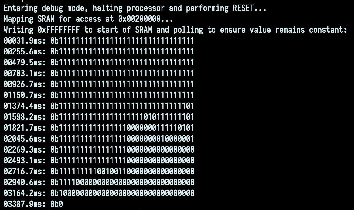
That looks an awful lot like something is wrong with the RAM! The bits are fading away to 0 quickly; which implies that either the bits weren’t written correctly, or they were written but they’re being read incorrectly, or maybe the chip is slowly losing power.
Reading More Closely #
As it turns out, one thing that could cause SRAM chips to behave like this is that one of three pins could be at the wrong voltage:
- the power pin, which is used to provide +3.3 volts
- the ground pin, which is used to provide, well, ground
- the “chip select” pin; which should be controlled by the CPU, but may have a pull-up resistor on it (as mentioned way at the top of this blog post).
With my oscilloscope, I was able to measure and find that:
- the chip was getting +3.3v on the power pin
- the chip’s ground pin was, indeed, ground
- the “chip select” pin was high at +3.3v all the time.
That last one was a bit suspicious; we’d expect that when memory accesses were happening, the chip select pin should go low, to indicate that the chip should be selected, even if only for nanoseconds at a time.
I took a peek at the resistor that had been installed, and took a look at its colour bands, which indicate the value of the resistor. I plugged them into an online calculator, and found:

4.7Ω.
After all of this debugging, it turns out that the SRAM chip was properly connected and working; it was just never being enabled, because its chip-select pin was being held at +3.3V all the time. This resistor should have been something like 4.7kΩ, which would provide more resistance - enough resistance to allow the CPU to overcome this resistor when enabling the chip. I must have missed a single “k” when indicating the resistor value.
I pulled out a pair of snips, clipped the resistor off the chip, and:

It lives!
A Bunch of Knobs #
Now that the synth worked, there were a couple more problems to fix. Turning the knobs on the left side of the synth’s panel all caused the synth to “glitch out” - values on the screen would jump around wildly. This wasn’t a complete dealbreaker, but definitely made the synth hard to use. To figure out why this was happening, I had to go back to the schematics once more. The knobs that were glitchy seemed to share one thing in common: they were all connected to one chip: a CD4051 analog multiplexer, labeled U27.

The Andromeda might be controlled by a digital CPU, but a lot of it is surprisingly analog. In fact, the analog signal from each knob on the front panel is sent all the way through to the main circuit board via a neat method called an analog multiplexer. Each potentiometer (knob) is connected to one multiplexer chip, which is essentially a controllable digital switch. The main CPU drives seven signals: POT_MUX_SEL[0-3], along with POT_ADDR[0-2]. Only one of the four POT_MUX_SEL signals are active at once, while the three POT_ADDR lines encode 3 bits of data, and thus have 8 possible values; putting these together allows the CPU to select between 32 different potentiometers whose values can be sampled. The analog multiplexers that sit on these lines are, well, analog, which means that even though they’re controlled by a digital address bus, their output is completely analog, allowing for extremely high fidelity.
A quick aside; what’s the difference between an analog and a digital synthesizer? Alesis claims in the Andromeda manual:
An analog instrument uses electronic circuitry for sound creation and filtering that is not dependent on its computer chip. While the instrument’s processor provides many control and memory functions, the basic sound path is in the hardware that is separate from the microprocessor.
This is true; but the line is somewhat blurred in the Andromeda, as the analog circuitry is controlled by a digital processor, whose inputs and outputs are 16-bit numbers.
In the 1990s when this synthesizer was developed, most synthesizers used 8-bit resolution for their parameters; each knob only had 28= 128 “steps,” which caused noticeable stair-stepping when turning knobs. (To think of this geometrically: if you turn a knob by less than about 3º, its value wouldn’t change due to this low resolution.) This led people to associate “digital” synthesis with “audible stair-steps when turning a knob.”
However, the designers of the Andromeda took a lot of care to keep all of the signals as analog as possible for as long as possible. As such, these front panel knobs send their analog values to the main board, where they’re then turned into digital values at the fairly high resolution of 16 bits, providing 65,536 possible steps. To put this in geometric terms again: if 8-bit synthesizers provide one step per 3º of rotation, the Andromeda provides one step per 0.0055º of rotation. That’s enough resolution to only be noticeable if you were to attach a 100-meter stick to each knob; at that scale, the far end of the stick would still move only about one centimeter per step. And with the number of parameters available on the synth, this level of detail means that there are approximately 2.4x10462 different unique combinations of sounds that could be made - 1.5x10231 times more than if the designers had used 8-bit parameter resolution.
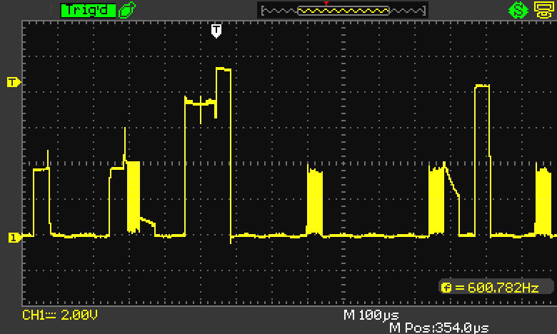
So. If the Andromeda uses analog multiplexers to send its front panel values on to the main CPU, what could be causing those values to be glitchy? Well, let’s take a look at the analog value using an oscilloscope.

Wow! This is kind of neat - we can see the multiplexing happening visually. Each of the “towers” in this visual “skyline” are the values of different knobs; with knobs turned all the way up being higher on the graph. If this was working correctly, we’d expect to see solid, flat values all along the graph. Seeing spikes, slopes up or down, or noisy values all indicate that something is wrong here; and sampling any of those values will probably result in the CPU thinking that some knobs are moving, even when they’re not.
Of particular interest here are the solid yellow sections of the graph, which indicate that values are moving up and down so quickly that they look like noise. Let’s zoom in on one of those:

Oof, that’s pretty bad. The value of this signal seems to be oscillating, which will make the CPU think that we’re turning this knob back and forth all the time. It’s hard to tell why this might be happening: this could be a broken multiplexer chip, or it could be one or more other broken chips causing bad signals to go into a multiplexer chip.
To debug this, I went ahead an ordered a brand new multiplexer chip for the low price of $0.66 (plus shipping). Unlike my last soldering job, this chip was big enough that I could replace it myself. (One gotcha: the chips on this board weren’t just soldered in place, but were also glued in place from underneath, causing me to rip up a couple traces despite my best attempts to be careful.)

However, after installing this new chip, the problem wasn’t quite resolved: the new signal was even dirtier than before! The oscillation hadn’t stopped, the signal had more overall noise, and some values are now sloping down instead of remaining constant:
Let’s go back to the drawing board a bit. The schematic shows that this multiplexer is connected to four knobs on the front panel, as well as two other signals that I hadn’t tested, labeled PITCH and MOD.

These two signals come from the pitch and modulation wheels at the left side of the keyboard; they’re both potentiometers, but attached to large vertically-mounted wheels that can be used more easily during performance. Let’s trace the schematic a bit more to find out where those signals actually come from, and how they’re generated.

It looks like the “raw” signal from the pitch and modulation wheels goes through another chip - an operational amplifier, or op-amp - which then amplifies its value to the 5V output by the other potentiometers.
This is where I’d show you a screenshot of my oscilloscope to illustrate how high the voltage was, or what signal was coming off of the op-amps here. However, I don’t have that screenshot, because instead, I touched the op-amp while the synth was powered up, and gave myself a mild burn. It was red-hot.

The op-amp chip - a TL082 - was supplied by two voltage rails: one at -15V, and one at +15V, making the maximum voltage across the chip a huge 30 volts. (Huge is relative here; but for a synth with many components that operate at 3.3V, this is a problem.) An op-amp has no business getting this in a correctly-functioning circuit. My best guess is that this component failed on its own, or may have failed catastrophically when I accidentally plugged in the cable between the front panel and main board backwards at one point.
Either way, this chip had to go. Not only was it causing instability in other chips, it was also sinking a ton of power and could have been a fire hazard or a danger to other parts of the circuit. Rather than trying to desolder it this time, though, I just cut it off with a pair of snips.

And with that, even without a new op-amp in place, the glitches were gone! Soldering in a new op-amp was pretty simple, but the result was great: all knobs worked again, including the pitch wheel and ribbon controller. The moral of the story: don’t plug cables in backwards when working on delicate analog electronics.
The Conclusion #
Well, thirteen months and hundreds of dollars later, my impulse buy is now a fully-working, beautiful-sounding, ultra-rare synthesizer. I still have a couple things left to do - replace some missing knobs, get replacement side panels made, fix some dead LEDs, fix the mod wheel, and replace some yellowed and scratched keys - but the hard parts of the project are done.
What was the root cause of the failure? Well, despite the many twists and turns along the way, it certainly looks like the Andromeda’s CPU was just dead. A full CPU replacement was enough to kick it back into life. Second to that, the data in the flash ROM may have been bad, but it’s very hard to tell if that would have been a blocker. The other issues (broken SRAM, blown op-amp, bad multiplexer) were all caused by my own attempts to repair the Andromeda without having its CPU replaced.
What if I’ve got a broken A6 Andromeda?
Having gone through this ordeal, I would suggest trying the following repair tips in order:
- If you’ve got an Arduino and are handy with software, open up your Andromeda and use my
arduino-coldfire-bdmPython library to try to connect to your Andromeda’s CPU over its debug port. From there, you’ll be able to see if the CPU is working and will be able to re-flash the firmware without buying any expensive equipment.- If that fails, try the simple fixes listed above: replace the oscillator on the LCD (a $3 part that’s easy to solder) or try turning the power off and on quickly to see if a pull-up resistor across the SRAM chip would make a difference.
- If that fails, buy a new MCF5307AI90B CPU online and replace it. It’s very difficult to do that without advanced soldering skills; you should send your Andromeda’s main board to Daniel Wynne at VideogameRepairs.ca. My repair bill came out to about $200 USD, but yours would likely be cheaper.
- Whatever you do, don’t flip the cable that connects the front panel to the main board. This will blow an op-amp and maybe an analog multiplexer on the front panel - at the very least - and you’ll wind up with some non-functioning and glitchy knobs.
If you’ve got an Alesis A6 Andromeda that’s in need of repair, stuck at the splash screen, not booting up, glitching out, or otherwise in a bad state: feel free to get in touch, as I’m apparently a qualified Andromeda repair technician now.
Was it worth it? I definitely came out ahead, ignoring my own labour costs. As of 2022, Andromedas are selling on the second-hand market for somewhere between $3,000 and $5,000, according to Reverb:

But does that mean I’ll be selling this synth? We’ll see. It’ll take a while to decide if this one-of-a-kind synth, which I put so much time into restoring, is worth getting rid of. (Maybe I’ll make a VST out of it instead. 👀)
Thanks to Paul Lamere, Zameer Manji, Eric Evenchick, and Sudara for reviewing drafts of this post.